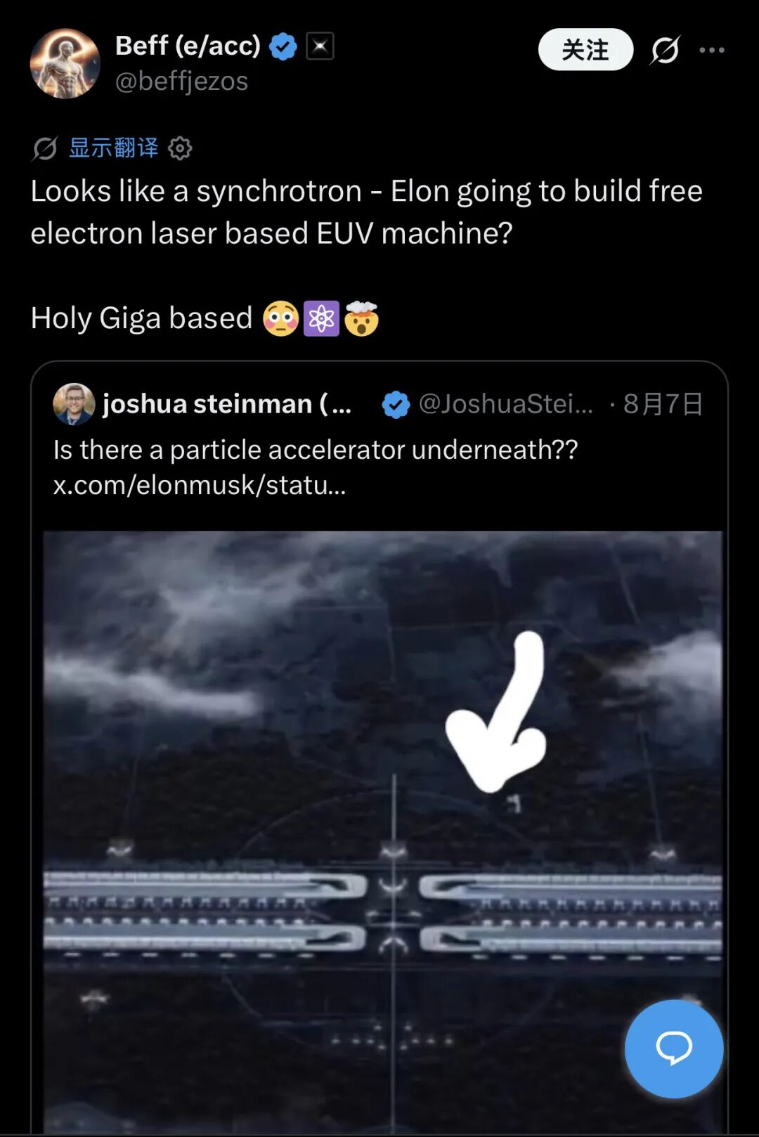
The story starts with a single social media post.
Recently, a tech blogger claimed that information released by TeraFab suggests Musk may be pursuing a Free-Electron Laser (FEL) approach — potentially challenging the dominance of conventional EUV lithography. Musk’s subsequent reply appeared to lend some credibility to the speculation.
And this is not entirely coming out of nowhere.
In March 2026, Tesla announced plans to work with SpaceX and xAI on TeraFab, a chipmaking project targeting 1 terawatt of AI computing capacity per year. On August 6, the project officially broke ground in Grimes County, Texas, with an initial investment of $16.8 billion. According to the plan, TeraFab will be a vertically integrated semiconductor facility covering the entire process, from chip design and manufacturing to packaging and testing.
But there is one major question: Where will the lithography machines come from?
ASML’s EUV lithography systems typically have lead times of more than 12 months, while the global supply of EUV machines is effectively dominated by ASML. If Musk chooses to simply wait for ASML’s production slots, TeraFab’s target of beginning production in 2027 could be extremely difficult to meet.
FEL could be the secret weapon that allows Musk to bypass that bottleneck.
Free-Electron Lasers (FELs) are hardly a new technology.
The basic principle is relatively straightforward: electrons traveling close to the speed of light pass through a periodically varying magnetic field, generating laser light. Unlike conventional EUV light sources, FELs can theoretically tune their output wavelength by adjusting the electron-beam energy, undulator period, and magnetic-field strength — potentially covering everything from soft X-rays to EUV and longer wavelengths.
To put it in admittedly imperfect terms: ASML’s Laser-Produced Plasma (LPP) EUV source is like a lithography tool with a fixed focal length, while an FEL is more like an optical system whose wavelength can be adjusted on demand.
The potential performance gap is even more striking.
ASML’s LPP-based EUV light source has an overall wall-plug efficiency of only around 0.05%, requiring roughly 4.4 MW of electrical power to generate 1 kW of usable EUV light. By comparison, advanced energy-recovery linac FELs (ERL-FELs) could theoretically produce 1 kW of EUV output with around 0.7 MW of electrical power, implying roughly six times higher efficiency.
FELs can also potentially deliver laser output in the kilowatt to tens-of-kilowatts range, far beyond the sub-1-kW power level associated with today’s EUV light sources.
Musk is not the only one betting on the potential of FELs.
U.S. startup xLight is pushing to commercialize free-electron-laser technology for EUV lithography. The company has raised $40 million in Series B funding, with former Intel CEO Pat Gelsinger serving as its executive chairman.
xLight’s vision is to use a single FEL source to power as many as 20 ASML lithography machines, with an operating lifetime of up to 30 years. The company claims the technology could cut wafer costs by around 50% while reducing capital and operating expenditures by more than threefold.
The U.S. Department of Energy has also entered the picture.
In August 2026, a U.S. startup received a Genesis Mission award from the Department of Energy for a project aimed at using X-ray lithography technology to challenge ASML’s position in the industry.
But there is still a very long road before FEL can truly disrupt EUV lithography.
The biggest challenge is engineering and commercialization.
ASML’s EUV light-source technology has gone through decades of development and now sits within a mature industrial ecosystem — with stability, reliability, high-volume manufacturing, and yield control all built into the system.
FELs, by contrast, typically require large-scale electron accelerators, undulators, vacuum systems, beam-control systems, and other highly complex infrastructure. The resulting systems can be enormous and extremely expensive.
xLight has secured significant funding, but its timeline for full commercialization remains uncertain.
There is another challenge: the shorter the wavelength, the harder everything gets.
Even if FEL technology reaches commercial deployment, moving from 13.5 nm toward shorter wavelengths introduces increasingly difficult problems involving optical systems, masks, photoresists, reflectivity, photon scattering, and other aspects of the lithography process.
Every step toward shorter wavelengths pushes the boundaries of what is technically and economically feasible.
ASML’s EUV lithography machines represent one of the semiconductor industry’s most formidable technology barriers of the past two decades.
But if the FEL route can be made to work at scale, that barrier may no longer be as impenetrable as it once seemed.
For Musk, TeraFab is essentially a massive technological bet — a bet that he can bypass ASML by pursuing an alternative architecture; that FEL technology can move from the laboratory into a high-volume fab; and that the economics of semiconductor manufacturing can be fundamentally redefined.
The stake: $16.8 billion.
The opponent: a Dutch giant that has dominated the lithography industry for two decades.
If the technology works, it could reshape the economics of advanced chipmaking. If it doesn't, the scale of the bet makes the downside equally dramatic.
That, in many ways, is classic Musk.

AI Market Research & Consumer Insights Provider
China's Leading Treasury Management Software Provider
AI落地解决方案及数字化创新服务提供商
A high-tech enterprise integrating product design, R&D, sales, and services.
Leading full-scenario data intelligence service provider in China.